Chip plays an important role in the high-end industries, such as smart phone, computer, home appliances, GPS device, etc. And the core device that makes the chip is generally dominated by the foreign manufacturers.
A few applications of semiconductor materialsStepper is a mask exposure system. By using laser source to etch the surface protective film of the wafer, circuit will be formed with data storing function. Most of the steppers adopt excimer laser which can produce deep UV laser beam. The leading and major excimer laser manufacturer Cymer was acquired by ASML. And the new stepper would be EUV stepper which can realize process of below 10nm. But this technique is now still dominated by the foreign companies.
But it is expected that China is gradually making breakthrough in chip making and later on realize self-production and mass production. Domestic steppers are also foreseeable and by then, the demand of high precision laser source will be increasing.
Another wide application of semiconductor materials is PV cell industry which is the fastest growing clean energy market with best potential in the world. Solar cells can be divided into crystalline silicon solar cell, thin-film battery and III-V compound battery. Among these, the crystalline silicon solar cell has the widest application. Opposite to laser source, PV cell is a device that transmits light to electricity. Photoelectric converting rate is the standard to tell how good the PV cell is. The material and process technique in this area is quite crucial.
In terms of cutting silicon wafer, traditional cutting tool was used, but with low precision and low efficiency and low yield. Therefore, many European countries, South Korea, the United States have already introduced high precision laser technique a long time ago. For our country, our production capacity of PV cell has reached half of the world. And in the past 4 years, as the PV industry has continued to grow, laser processing technique has gradually been used. Nowadays, laser technique is contributing to the PV industry by performing wafer cutting, wafer scribing, grooving of the PERC battery.
The third application of semiconductor is PCB, including FPCB. PCB, which is the key component and the basis of all electronics, uses a large amount of semiconductor materials. In the past few years, as the precision and integration of PCB becomes higher and higher, tinier and tinier PCB will come out. By then, traditional processing and contact processing device will be hard to adapt, but laser technique will become more and more used.
Laser marking is the simplest technique on PCB. For the time being, people often use UV laser to perform marking on the surface of the materials. Laser drilling, however, is the most common technique on PCB. Laser drilling can reach micrometer level and can perform very tiny hole that mechanical knife couldn’t do. In addition, copper material cutting and fixed fusion welding on PCB can also adopt laser technique.
As laser enter micro-machining era, S&A Teyu promoted ultra-precise air cooled water chillerLooking back the laser development in the past few years, laser has wide applications in metal cutting and welding. But for high precision micro-machining, the situation is the other way around. One of the reason is that metal processing is kind of a rough machining. But high precision laser micro-machining requires high level of customization and faces challenges like difficulty of developing this technique and lots of time spent. Nowadays, high precision laser micro-machining is mainly involved in consumer electronics like smart phone whose OLED screen is often cut by laser micro-machining.
In the coming 10 years, semiconductor material will become a priority industry. Semiconductor material processing could probably become the stimulus of the rapid development of laser micro-machining. Laser micro-machining mainly used short-pulsed or ultra-short pulsed laser, also known as ultrafast laser. Therefore, with the trend of domestication of semiconductor material, the demand of high precision laser processing will increase.
However, high precision ultrafast laser device is quite demanding and it needs to be equipped with equally high precision temperature control device.
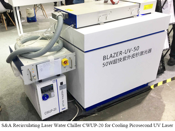
To meet the market expectation of domestic high precision laser device, S&A Teyu promoted CWUP series recirculating
laser water chiller whose temperature stability reaches ±0.1℃ and it is specifically designed for cooling ultrafast lasers like femtosecond laser, nanosecond laser, picosecond laser, etc. Find out more information about CWUP series laser water chiller unit at
https://www.teyuchiller.com/portable-water-chiller-cwup-20-for-ultrafast-laser-and-uv-laser_ul5


